Nana Sutisna, S.T., M.T., Ph.D.
STEI ITB
Abstrak
With the increasingly important role of semiconductor technology, especially in the digital era, human resource competency in this field is essential. However, the fulfillment of human resources in the semiconductor field, especially IC design is currently still lacking. As a result, there is a significant gap between the actual needs in the industry and the skills students acquire in lectures. One of the competencies that need to be developed in addition to a fundamental understanding of chip technology, including design concepts, another factor that must be possessed is mastery of CAD (Computer Aided Design) tools in every design stage (design flow) that follows state-of-the-art CAD technology.
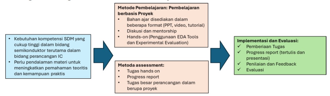
Therefore, a learning method is needed that can facilitate students to gain real experience in the chip design process using CAD tools or the latest methodologies, either based on open source technology or licensed commercial ones. In this research, a teaching material will be developed to support Student Centered Learning (SCL) based learning activities that can be applied to lectures related to IC design, both digital, analog or mixed-signal ICs. The teaching material developed is in the form of tutorial modules and hands-on projects, which cover the design process, implementation and testing/verification of chip designs.
Kata Kunci: Semikonduktor, IC Design, Student Centered Learning, Project Based Learning
Pendahuluan
Today, almost every digital or electronic device in everyday life relies on semiconductor components, specifically chipsets. Furthermore, to support future technological developments such as artificial intelligence (AI), electric vehicles, green energy, cloud computing, 6G, quantum computing, and various other emerging technologies, semiconductor technology is crucial. With the increasing importance of semiconductor technology, especially in the digital era, human resource competency in this field is essential.
Although the demand for human resources in the semiconductor sector, particularly IC design, is increasing, this human resource requirement is still insufficient. There is still a significant gap between the actual needs in industry and the skills students acquire in lectures. One of the competencies that need to be developed, in addition to a fundamental understanding of chip technology, including design concepts, is mastery of CAD (Computer Aided Design) tools in every design stage (design flow) that follows state-of-the-art CAD technology. Therefore, a learning method is needed that can facilitate students to gain real-world experience in the chip design process using CAD tools or cutting-edge methodologies.
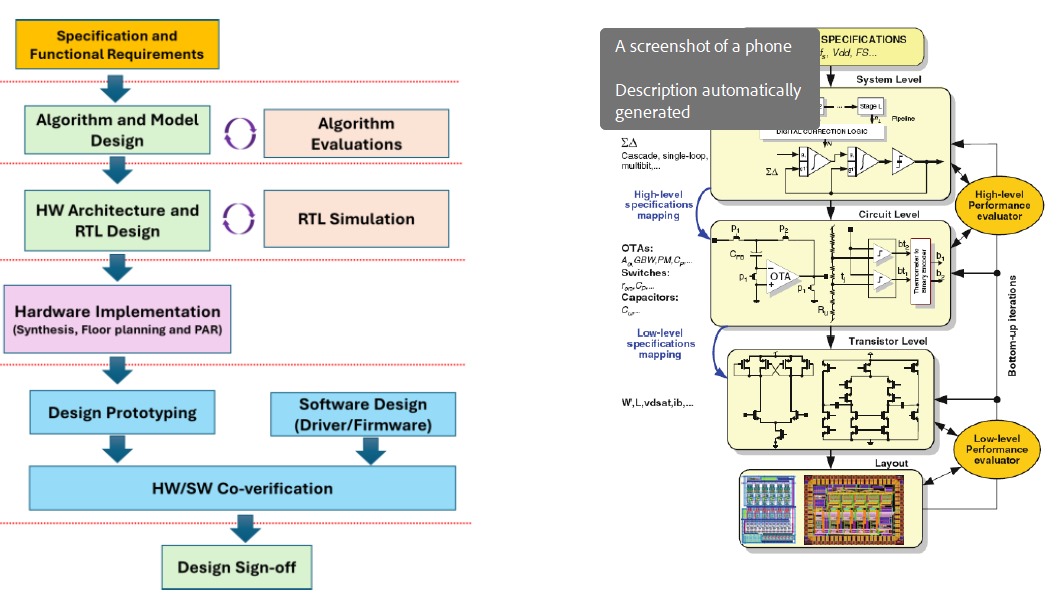
Integrated Circuit Design Flow (Digital and Analog)
Pengembangan Metode Pembelajaran
Output: College Syllabus (Project-based Learning)
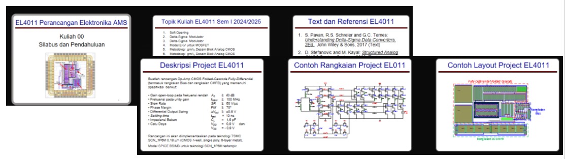
Modul Tutorial CAD Tools Cadence

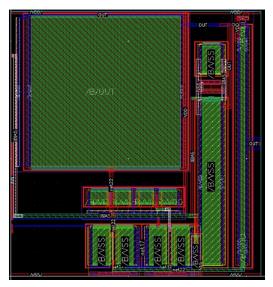
Chip Layout Op-Amp
Kesimpulan
special approach has been designed for IC design learning using project-based learning to increase the level of achievement of CPMK fulfillment and student competency by using industry-standard methodologies and CAD tools.