Muhammad Amin Sulthoni
STEI-ITB
Akhmadi Surawijaya
STEI-ITB
Dini Nur Farida Putri
STEI-ITB
Abstract
Transparent thin- ilm material has unique characteristic when used in making solar cells. Transparent thin-film material will transmit some photon energy and less are reflected. To be able to maximize energy absorption in solar cells so that the energy transmitted by the thin-film material is not wasted, it can be stacked with solar cells of other materials whose absorption spectrum is different from the absorption of the thin-film material. By knowing the optical and electrical characteristics of each material, it is hoped that can determine the pairing of thin-film materials and other materials. In this research, an optical simulation will be carried out using the Lumerical FDTD simulator. By using this simulator, the re lection, transmittance, and absorbance spectrum of a material can be determined. This simulation was carried out on several materials including Crystalline Si, GaAs, InAs, GaAs-InAs, CdS, CdTe, CdS, and Perovskite. Some of these materials will be simulated at thicknesses of 2.0 μm, 1.75 μm, 1.5 μm, 1.0 μm, 0.8 μm, 0.5 μm, 0.2 μm, 0.1 μm, and 50 nm. The thicker the material used, the greater the absorbance obtained and the greater the short circuit current. Of the six materials used, the highest spectrum absorbance value for the CdS material by 80% up to 520 nm, Perovskite material reaches 80% up to 550 nm wavelength, followed by CdTe at 75% up to 780 nm wavelength, then GaAs-InAs and InAs at around 67%.
Keyword: Research 1, Research 2, Research 3.
Introduction
There are 2 types of solar cells currently available, namely crystalline silicon and thin film. Thick film crystalline silicon usually ranges from 1 – 100 micrometers. Meanwhile, thin film is generally below 1 micrometer. With the thin film, the solar cells that are successfully made can be transparent so that the reflectance index is low. This low reflectance index greatly influences the amount of photon energy that enters the active layer material and can be transmitted to the solar cells below with minimum energy reflection.
In this research, we will observe the optical and electrical characteristics of several materials for active layers such as thin film and thick film semiconductors and organic solar cells, the influence of the thickness of the active layer of solar cells, the impact of several materials and thickness of the anti-reflective coating, and the influence of stacking of 2 active layers with different materials.
It is hoped that by knowing the optical and electrical characteristics and properties of each material and their effect on various thicknesses and combinations, we can determine and conclude the combination of material types and thicknesses to obtain the most optimal solar cell performance and efficiency.
Research Method
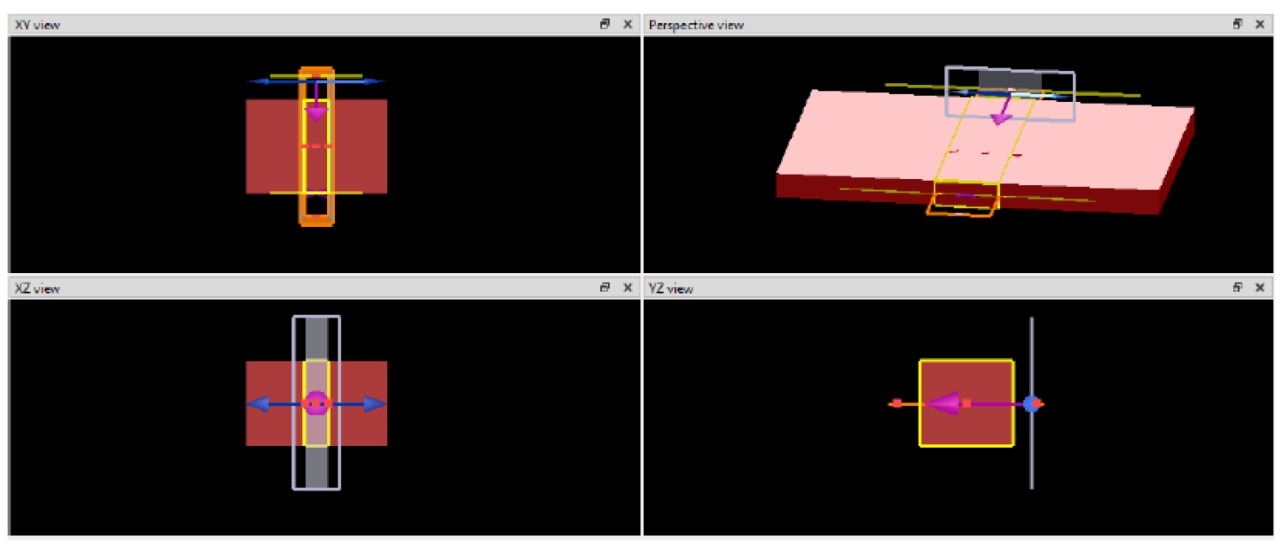
The Lumerical FDTD simulator will be used in this study to conduct an optical simulation. This simulator can determine a material’s reflectance, transmittance, and absorbance spectrum. By design, it is possible to position a monitor just below the material to detect the spectrum transmitted by it, and above the light source to serve as a reflectance monitor. Only the spectrum reflected by the material is recorded, not the combination of the reflection and the source, because the reflectance is not positioned between the source and the material being studied.

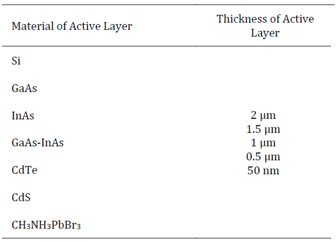
Several materials were used in this simulation, including crystalline silicon, III-V group semiconductor, thin-film, and organic. We’ll replicate a few of these materials in different thicknesses. Afterwards, covering the active layer material with an anti-reflectance layer such as MgF2, SiN, SiO2, TiO2, and Al2O3. A table listing the various iterations of the experiments that will be conducted is provided below.

Discussion & Result
As can be seen from result figures, it can be seen that the thicker the material used, the greater the spectrum of light absorbed by the material. Despite the greater amount absorbed, the absorption curve looks more oscillating. This is due to the lattice characteristics of each material.


Since the best absorbance results are at a thickness of 2 microns, the next comparison will use materials with a thickness of 2 microns. The absorbance obtained increases with material thickness. CdTe is the material that absorbs light spectrums the best out of the seven material samples that were used. At a wavelength of 300 to 780 nm, CdTe exhibits a fairly constant absorbance value, reaching 75%.
However, for combining two solar cell materials to obtain maximum absorbance, perovskite is the best choice. Perovskite can absorb up to 80% but only up to a wavelength of 520 nm. So, to maximize absorption, a material that can absorb well at wavelengths above 520 nm is needed. The second material for perovskite is GaAs-InAs. GaAs-InAs material has a constant absorption of 67% at high wavelengths.
Conclusion
The thicker the material, the greater the absorbance obtained. Of the 7 material samples used, the best material in the absorption of the light spectrum is CdTe. CdTe has a fairly constant absorbance value at a wavelength of 300 to 780 nm with an absorbance value reaching 75%.
The most optimal combination of 2 materials to obtain the maximum absorbance is to use perovskite and GaAs-InAs materials. But to get solar cells with these materials is difficult, so for further research it is recommended to use CdTe and Silicon materials that are already sold in the market.